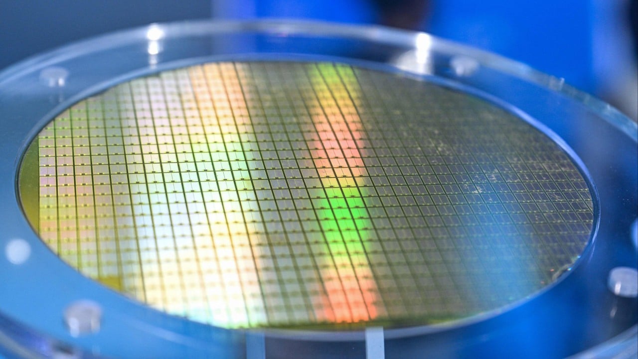
YMTC Backed Capital Targets Silicon Alternatives to Dodge Washington Curbs
State-backed venture funds tied to Yangtze Memory Technologies Corp are quietly steering capital toward unconventional semiconductor manufacturing paths to bypass strict American export controls. When Washington slammed the door on extreme ultraviolet lithography access, Beijing memory architects did not slow down. They redirected capital. A venture vehicle anchored by the state memory titan has poured fresh funding into alternative chipmaking architectures, specifically targeting non-traditional fabrication routes that sidestep Western intellectual property entirely.
For years, the semiconductor playbook was rigid. Scale down transistors, buy lithography machines from ASML, and stack silicon. That blueprint is broken. American trade restrictions designed to lock China out of advanced node production have instead forced a massive reallocation of domestic resources. By backing startups experimenting with non-standard materials, packaging breakthroughs, and mature-node workarounds, YMTC and its financial partners are constructing an entirely parallel supply chain. For a deeper dive into this area, we recommend: this related article.
The Mechanics of State Directed Venture Capital
Venture capital usually follows profit margins. State-directed capital in China follows national survival. When a memory giant like YMTC backs early-stage alternative manufacturing ventures, the objective is not immediate quarterly returns. The goal is structural insurance.
Consider the constraints. Standard immersion lithography tools available to Chinese fabs hit a hard physical wall at the 28-nanometer and 14-nanometer thresholds without multi-patterning techniques that drive up costs and drop yields. To escape this trap, investors are looking at physics outside the conventional silicon box. This includes advanced packaging techniques that stitch together smaller, cheaper, mature-node chiplets to rival the performance of monolithic processors fabricated on cutting-edge nodes. For broader background on the matter, extensive reporting can also be found at Mashable.
Financial filings and regional registry data reveal a methodical pattern. Investment arms linked to YMTC have quietly taken stakes in firms specializing in photonic interconnects, novel substrate engineering, and alternative deposition tools. These are not headline-grabbing mega-rounds. They are quiet, strategic injections of liquidity designed to keep domestic research alive while export restrictions tighten further.
Why Mature Nodes Are Getting a Brutal Makeover
The narrative that China is completely paralyzed by semiconductor sanctions ignores the engineering reality on the ground. Mature nodes are receiving a brutal makeover. Instead of obsessing exclusively over sub-7-nanometer shrinks, domestic labs are optimizing what they already own.
Advanced packaging is the immediate battleground. By vertically stacking memory and logic dies using hybrid bonding methods pioneered by companies like YMTC in their Xtacking architecture, engineers can squeeze massive bandwidth out of older manufacturing lines.
The Chiplet Strategy
- Vertical Integration: Stacking functional layers instead of shrinking individual transistors on a single die.
- Yield Preservation: Smaller dies yield better percentages per silicon wafer, bypassing the catastrophic defect rates seen on early-stage experimental nodes.
- Hardware Independence: Reducing reliance on extreme ultraviolet scanners by relying on mature deep ultraviolet tools combined with clever design topology.
This approach changes the economics of production. It trades raw lithographic brilliance for architectural ingenuity. While American policy makers focused on starving Chinese fabs of EUV machines, they underestimated the capacity of domestic engineers to innovate around the bottleneck through sheer packaging density.
The Bottlenecks No One Wants to Discuss
Throwing billions of yuan at alternative manufacturing routes does not guarantee success. Physics remains stubborn.
Alternative materials and advanced packaging carry severe thermal and electrical penalties. When you stack silicon dies tightly together, heat dissipation becomes a nightmare. Without high-end thermal interface materials and precise cooling designs, performance throttles rapidly under load. Furthermore, domestic toolmakers are still playing catch-up in critical auxiliary segments like chemical mechanical planarization and specialized metrology.
Supply chain fragmentation also plagues these alternative routes. Even if a startup invents a brilliant method for non-silicon channel routing, scaling that process from a university-adjacent cleanroom to a high-volume manufacturing line requires an ecosystem of chemical suppliers, equipment maintainers, and testing facilities that simply do not mature overnight.
The Geopolitical Fallout
Washington is watching these workarounds closely. Bureaucrats in the Department of Commerce are already debating whether current rules are too narrow, focusing strictly on lithography while ignoring the software, packaging, and alternative material spaces where Chinese capital is now concentrating.
Closing these loopholes will not be simple. Once capital flows into foundational research and diverse manufacturing paths, it disperses across a decentralized network of private and semi-private entities. You cannot sanction an entire ideology of self-reliance. Every tightening of the regulatory screw merely accelerates the domestic push toward technological autarky, forcing local firms to rely less on Western imports and more on indigenous breakthroughs.
The semiconductor cold war has entered its second phase. The first phase was about blocking access to existing tools. The upcoming phase will be fought over whether alternative architectures can scale fast enough to render those blocked tools obsolete.