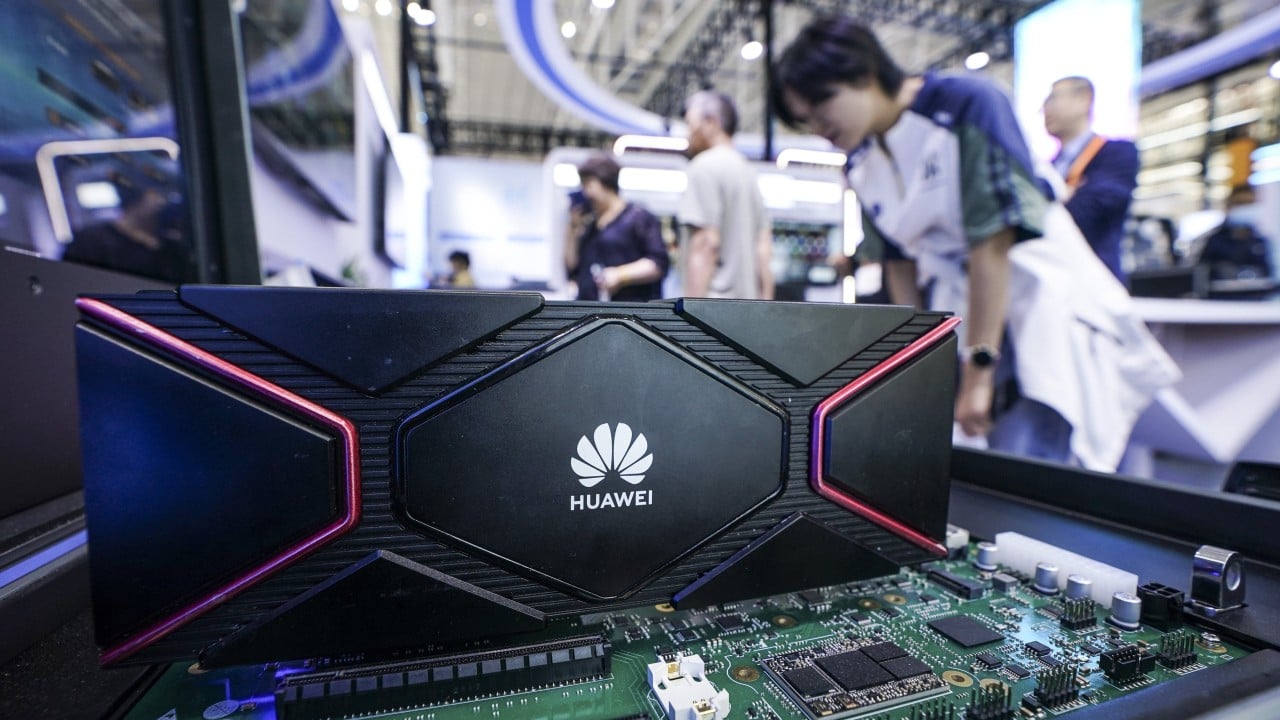
Huawei has officially abandoned the traditional race to shrink transistors, unveiling an architectural pivot designed to neutralize Western export controls and achieve performance parity with global leaders. Dubbed the Tau Scaling Law, the methodology ditches geometric miniaturization in favor of temporal optimization. Instead of relying on extreme ultraviolet lithography to pack more transistors into a flat plane, the strategy optimizes signal propagation speed across three-dimensional spaces. By compressing internal wiring through an intra-die vertical architecture called LogicFolding, the company claims it will deliver high-end chips with a transistor density equivalent to a 1.4-nanometer node by 2031, with the first commercial iterations arriving in flagship Kirin smartphone processors this autumn.
The initiative represents a fundamental shift in the geopolitical tech war. For years, Western sanctions assumed that blocking China from purchasing ASML's advanced extreme ultraviolet (EUV) machines would cap domestic semiconductor capabilities at the 7-nanometer or 5-nanometer threshold. This thesis underestimated architectural adaptation. The industry is witnessing a structural workaround that shifts the metric of success from physical feature size to system-level latency reduction.
The Ghost in the Lithography Machine
To understand why this approach matters, one must look at the physical brick wall Western chip designers are hitting. For half a century, the industry marched to the drumbeat of geometric scaling. Shrink the gate, thin the wire, pack them tighter.
Yet, as the global market approaches sub-2-nanometer thresholds, the physics of conventional silicon are breaking down. Quantum tunneling causes electrons to bleed through ultra-thin barriers. Interconnect resistance skyrockets as copper wires narrow to atomic widths, turning paths into thermal bottlenecks. The industry has been spending exponentially more money to achieve diminishing returns in clock speed and power efficiency.
Huawei is turning these headwinds into an insulation strategy. Because U.S. export controls permanently cut off access to top-tier lithography, continuing down the traditional road was a dead end. The company pivoted from the physical geometry of the gate to the time constant, denoted by the Greek letter tau ($\tau$).
$$\tau = R \times C$$
In physics, $\tau$ represents the product of resistance ($R$) and capacitance ($C$). It dictates the time required for an electronic signal to travel from one transistor to the next. If you cannot make the transistors smaller to reduce resistance, you must shorten the distance the signal travels.
Instead of spreading components across a massive 2D canvas, the LogicFolding framework folds the traditional circuit layout into a multi-layered vertical stack. This is not the standard multi-die packaging utilized by Nvidia or AMD, where separate completed chips are laid out next to each other on an interposer. This is true intra-die vertical logic stacking. The logic circuits themselves are split and folded across a dual-layer framework within a single piece of silicon.
The physical implications of this layout change are immediate.
- Total internal wire length drops significantly, with early academic prototypes from Peking University indicating up to a 30% reduction in critical path wiring.
- Shorter wires mean less resistive and capacitive load, allowing signals to propagate faster at lower voltages.
- Transistor density per square millimeter climbs without requiring tighter physical engraving from a lithography lens.
According to data presented at the IEEE International Symposium on Circuits and Systems in Shanghai, this structural compression yields a 53.5% increase in apparent transistor density for the upcoming 2026 Kirin smartphone processor, hitting 238 million transistors per square millimeter. That matches the density metrics of Western 3-nanometer processes, despite being fabricated on older, legally accessible manufacturing nodes.
The Software Weapon and the Yield Problem
A radical hardware blueprint is useless without an ecosystem to design and manufacture it. Standard electronic design automation (EDA) software, dominated by Western firms like Synopsys and Cadence, is built for 2D placement and routing. You cannot simply feed a 3D folded logic architecture into a traditional design pipeline and expect it to work.
To bridge this gap, China has spent the last several years constructing a parallel domestic toolchain. The recent unveiling of a native, true-3D EDA tool by Peking University’s School of Integrated Circuits shows how coordinated this push has become. The software treats the multi-layer structure as a single vertical design space from the very beginning, optimizing heat distribution and signal paths simultaneously.
Yet, the true test of this strategy will not occur in a university lab. It will play out on the factory floors of domestic foundries like SMIC.
Vertical logic stacking introduces immense manufacturing complexity. Aligning two layers of logic circuits at the transistor level requires nanometer-scale precision across the entire surface of a wafer. If the vertical interconnects fail to align perfectly, the entire chip is electronic waste.
Conventional advanced packaging already suffers from lower yields than monolithic manufacturing. Doing this at the intra-die logic layer amplifies the risk. Huawei claims it has quietly validated these principles over six years, designing and producing 381 chips across various industries using elements of this temporal framework. But mass-producing a high-yield flagship smartphone processor by the millions is an entirely different operational beast.
Thermal management presents another major hurdle. Stacking active logic circuits directly on top of each other traps heat in the lower layers. In an AI data center environment, where accelerators run at maximum TDP for days at a time, sub-optimal thermal dissipation leads to clock throttling or catastrophic hardware degradation. The 41% energy efficiency gain claimed by the LogicFolding architecture is intended to offset this thermal trap, but theoretical efficiency rarely translates perfectly to real-world deployment.
The Reconfigured Competitive Landscape
The market effects of this architectural pivot are already rippling through the supply chain. Just days before the formal announcement of the new scaling framework, Nvidia CEO Jensen Huang noted that his firm had largely conceded the Chinese AI market to Huawei. This was not a statement born of corporate defeatism, but a clear-eyed assessment of shifting domestic dynamics.
The Chinese market is rapidly consolidating behind native platforms. Tech giants and local cloud providers are no longer waiting for Washington to relax export rules on hobbled, export-compliant Western variants. They are migrating their workloads to the Ascend AI ecosystem.
This domestic alignment is creating an architectural lock-in. Silicon performance is only half the battle in modern computing. The software stack, the compiler efficiency, and the interconnect topology dictate true system capability. By standardizing on its UnifiedBus protocol, Huawei is building SuperPods with native memory semantics that cut latency across massive server clusters. It is an end-to-end stack replication of the exact strategy that made Nvidia dominant globally.
| Metric | Traditional Geometric Scaling | Huawei Tau Scaling Framework |
|---|---|---|
| Primary Variable | Physical transistor gate size ($nm$) | Signal propagation time constant ($\tau$) |
| Core Equipment Dependency | High-NA Extreme Ultraviolet (EUV) Lithography | 3D Intra-die EDA Tools & Advanced Bonding |
| Density Gains Via | Sub-atomic physical engraving | Vertical LogicFolding and wire compression |
| Main System Bottleneck | Gate leakage and quantum tunneling | Thermal dissipation and vertical alignment yield |
The competitive threat to global foundries is not that China will suddenly surpass TSMC in pure, native lithography sub-nodes. TSMC is actively tracking toward true 1.4-nanometer physical mass production by 2028, whereas Huawei's roadmap targets 1.4-nanometer density equivalence by 2031. Western engineering will retain the raw physical edge.
The danger for global players is economic decoupling. If China can deliver comparable system performance, processing speeds, and AI training throughput using mature lithography nodes wrapped in advanced vertical architectures, the premium for Western silicon disappears inside the world's largest hardware market. The high capital expenditure required to build leading-edge fabs in the West relies on global volume to sustain profitability. Lose the Chinese market entirely, and the economics of the traditional semiconductor roadmap begin to fracture.
Sanctions operate on the assumption that a competitor will stop running when you take away their paved road. They ignore the reality that the competitor might simply build a different vehicle designed for the terrain left behind. By anchoring its future to temporal scaling rather than physical miniaturization, Huawei has institutionalized an engineering path that bypasses the exact choke points Washington spent years establishing. The battle for silicon supremacy is no longer about who can print the smallest line, but who can move a bit of data across a three-dimensional circuit the fastest.