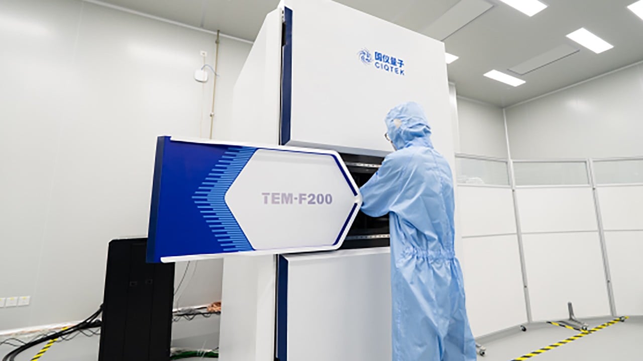
Seeing an individual atom used to be a privilege controlled by a tiny club of instrument makers in the United States and Japan. Now Hefei-based CIQTEK has rolled out the TEM-F200, a domestically developed 200-kilovolt field emission transmission electron microscope hitting a 0.1-nanometre information limit and a 0.25-nanometre point resolution.
That single milestone changes the conversation around scientific hardware. For years, semiconductor labs, battery researchers, and materials scientists outside the dominant Western and Japanese supply chains faced long lead times, steep import hurdles, and export-control anxiety whenever they needed serious atomic-scale imaging. A commercial-ready 200 kV field emission TEM built in China doesn't magically erase decades of incumbent engineering overnight, yet it signals a real shift from lab prototypes to factory-floor and research-lab deployment.
Let's be honest about what a headline like "0.1 nanometres" really means before anyone declares a winner. Spec sheets love big-sounding numbers, and microscopy specs are notorious for tripping up casual readers.
What the Electron Microscope Specs Actually Mean
When you read that a transmission electron microscope reaches a 0.1-nanometre information limit alongside a 0.25-nanometre point resolution, you're looking at two different benchmarks of clarity. Point resolution tells you the smallest distance between two distinct points you can tell apart directly in a standard image without heavy post-processing. Information limit goes deeper—it measures the finest spatial detail the instrument can transfer into the signal, which matters when researchers use phase reconstruction or analytical techniques to push past raw point-to-point contrast.
A 200-kilovolt acceleration voltage sits right in the sweet spot for many materials science, catalysis, and semiconductor failure-analysis tasks. Higher-voltage 300 kV columns are great for certain heavy or thick specimens, while lower-voltage setups help limit beam damage on delicate samples. A solid 200 kV field emission gun gives a bright, coherent electron beam capable of handling everyday workhorse characterization without requiring a massive facility footprint.
Still, specs on a datasheet are only half the story in electron microscopy. Real-world performance depends on mechanical vibration isolation, electromagnetic shielding, column stability over hours-long sessions, detector sensitivity, and how easily an operator can align the beam without spending half the day fighting drift.
Point Resolution vs. Information Limit in Plain English
Think of point resolution as whether your camera lens clearly separates two tiny streetlights side by side at night. Information limit is closer to whether subtle texture and fine detail still survive in the raw file so your software can pull out extra structure.
Neither number is fake or meaningless, yet mixing them up leads to bad comparisons. A system with a 0.25 nm point resolution and a 0.1 nm information limit is competitive in the workhorse tier, especially for an initial commercial generation, though top-end aberration-corrected instruments from long-established players still set steep bars in specialized sub-angstrom workflows.
Why US and Japanese Makers Held the Crown for So Long
If you've ever worked in a materials characterization lab, you know the names that usually sit on the column. Japanese firms like JEOL and Hitachi, alongside American-rooted leaders like Thermo Fisher Scientific (formed from FEI and Philips traditions), built deep moats over generations.
Those moats aren't built out of a single secret part. They come from decades of accumulated know-how across:
- High-voltage stability and ultra-low ripple power supplies that keep electron wavelengths steady.
- Precision electromagnetic lenses and aberration correctors machined to microscopic tolerances.
- Vacuum engineering that holds extreme low pressures without contaminating sensitive samples.
- Mature software ecosystems, automated alignment routines, and global field-service networks.
When a lab buys a multi-million-dollar electron microscope, it isn't just buying a tube that shoots electrons. It's buying uptime, calibration support, training, and parts availability when a vacuum valve or high-voltage feedthrough acts up on a Tuesday morning. Catching up on raw optics is hard; matching decades of service reliability and workflow software is just as tough.
Commercialization Changes the Real Equation
Unveiling a prototype at a conference—like CIQTEK's push around the TEM-F200—is a big deal, and moving toward commercialization is where things get real. In scientific instruments, going from "we built one that works in our demo bay" to "we can manufacture, ship, install, and support dozens of units for demanding customers" is where many ambitious hardware projects stall.
Domestic supply chain independence is a major driver behind this push. Semiconductors, advanced packaging, solid-state batteries, and novel alloys all rely on seeing tiny defects, grain boundaries, or interface layers before a batch fails in production. When geopolitical friction threatens cross-border equipment shipments or servicing, having a homegrown alternative reduces single-point dependency.
A commercial-grade microscope only proves its worth once independent labs run it day after day on messy, real-world samples—not just pristine calibration grids.
💡 You might also like: The $20 Billion Ticket to a Dead Silence
Even if domestic labs adopt a new Chinese 200 kV TEM first, the ripple effects reach global buyers too. Fresh competition puts pressure on pricing, delivery schedules, and upgrade cycles across the entire scientific instrument market.
Where Labs Still Trip Up on High-Resolution Imaging
I've seen plenty of teams blame their microscope when the real bottleneck was sample prep or lab environment. You can drop a world-class electron microscope into a room with poorly isolated floor vibrations, AC draft fluctuations, or stray magnetic fields from nearby equipment, and your crisp atomic lattice turns into a blurry smudge.
Sample preparation is another classic trap. Thinning a semiconductor wafer or battery cathode to electron transparency—often well under 100 nanometres—without introducing ion-beam damage or oxidation takes real skill. Many labs buy high-end imaging hardware while underinvesting in focused ion beam prep, clean sample transfer, or skilled operators.
Another mistake is chasing maximum resolution for every routine check. Sometimes a faster scan, better elemental mapping, or higher throughput matters far more than squeezing out every last picometre of theoretical limit.
Practical Next Steps If You're Evaluating TEM Gear
If you're leading a lab, planning a capital purchase, or tracking hardware competition in materials and semiconductor research, skip the hype and take a few concrete steps:
- Audit your actual bottlenecks first. Check whether your team is slowed down by instrument access, sample prep throughput, detector speed, or data analysis before shopping for a new column.
- Map required workflows to acceleration voltage and accessories. Confirm whether 200 kV fits your target materials and whether you need spectroscopic add-ons like EDS or EELS rather than paying for specs you won't use.
- Demand real application benchmarks on your own sample types. Ask any vendor—incumbent or newcomer—for test runs on materials similar to yours, plus clear details on maintenance intervals, spare parts, and local service response times.
- Budget for site readiness and operator training. Factor in room acoustics, vibration floors, magnetic shielding, and hands-on training hours, because those details decide whether your microscope hits spec every week.